تعداد اعضای رانندگان فعال به همراه کشنده در سیستم حمل و نقل بین المللی شرکت آرتمیس ترانس
0
سال های فعالیت
بیش از بیست سال فعالیت تخصصی در حوزه حمل و نقل بین المللی در کشور های اروپایی
0
قرارداد های موفق
بیش از صد قرارداد موفق واردات و فروش انواع کشنده و تریلی در ایران و کشور های اروپایی
0
کشنده های آماده فروش
تعداد کشنده و تریلی آماده انتقال با سند رسمی و محضری به صورت کارشناسی شده
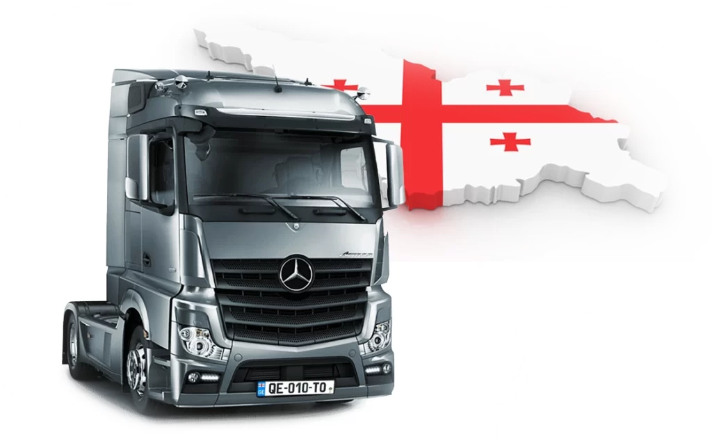
پلاک گرجستان
کشنده های پلاک گرجستان کشنده هایی هستند که مانند کشنده های پلاک ایرانی به راحتی میتوانند از ایران به کشور های مختلف بار حمل کنند . کشور گرجستان این امکان را برای همه مردم کشورهای مختلف داده است که بتوانند از هر جای دنیا از گرجستان خودرو یا کشنده بدون نیاز به اقامت یا شهروندی خرید کرده و صاحب ان بشوند. شرکت ارتمیس ترانس با واردات کشنده های پلاک گرجستان و ارائه خدمات باربری و ارائه انواع مدارک لازم برای حمل بار در خدمت مردم کشور عزیزمان ایران می باشد
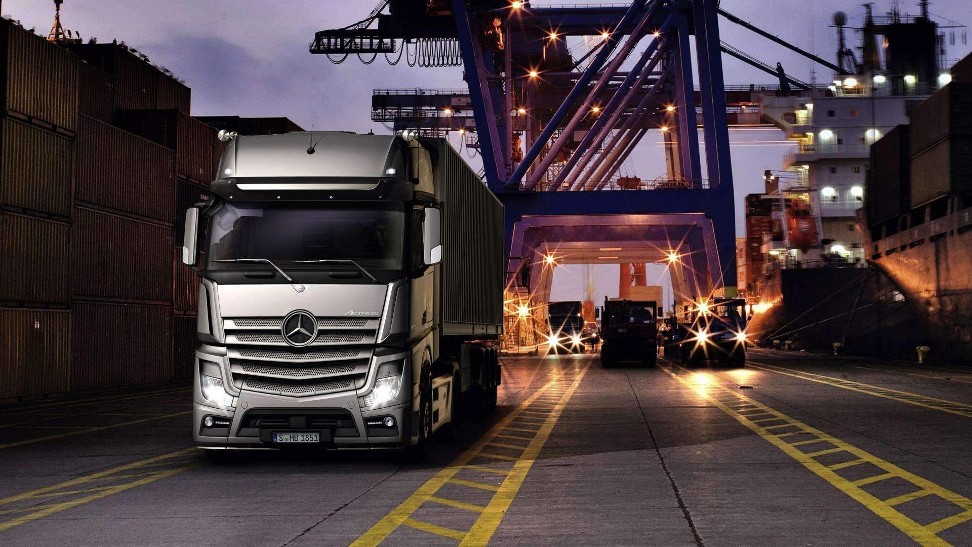
حمل و نقل
شرکت ارتمیس ترانس با داشتن بیش از 20 سال سابقه در حمل ونقل و همکاری با تاجران ایران از لحاظ موجودی بار بدون وقفه برای رانندگان بار و برای تاجران راننده و کشنده تامین کرده است که با توجه به صداقت و عمل به تعهد این شرکت محبوب تاجران و رانندگان مشتاق همکاری وانجام تجارت با این شرکت را داشته اند . از چند مورد تعهدات این شرکت میتوان به تعهد به تامین برای همه مشتریان و رانندگان خود . تعهد ارائه انواع مدارک لازم برای حملو نقل بار . تامین تعداد زیاد کشنده برای تاجران و پشتیبانی 24 ساعته برای همه رانندگان شرکت در همه مسیر ها و راه برای حمل بار اشاره کرد
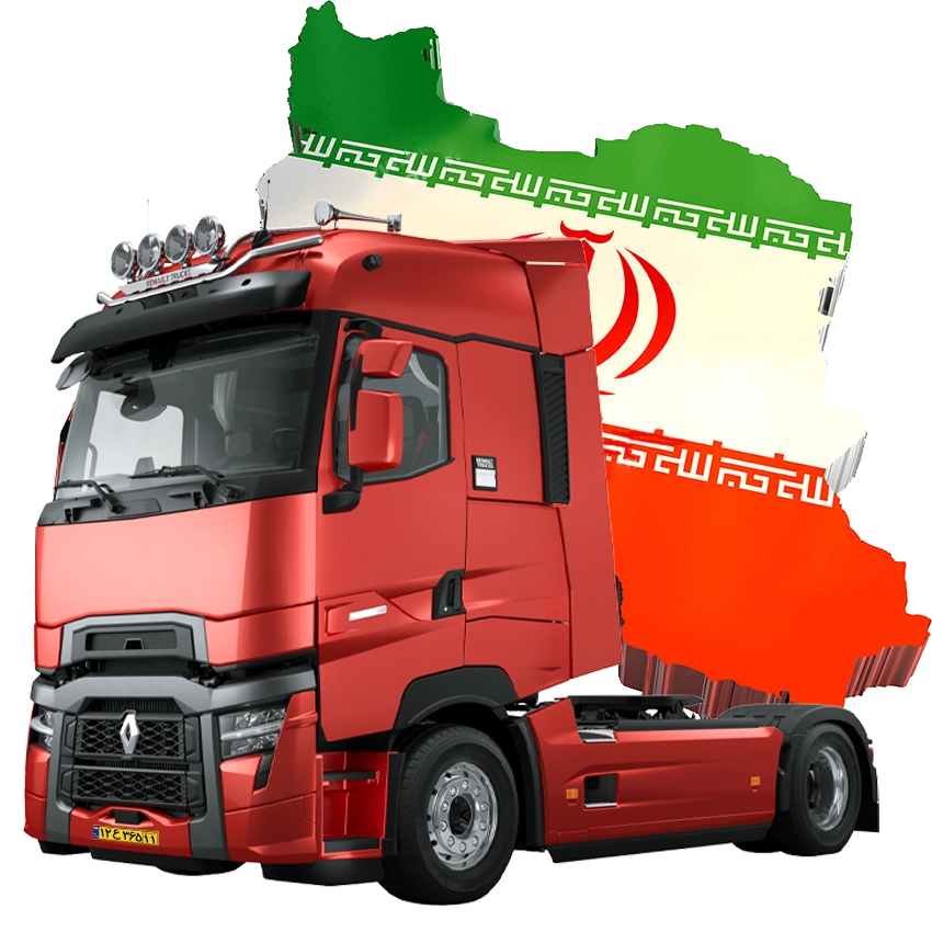
واردات کامیون های پلاک ملی
شرکت ارتمیس ترانس با داشتن نیرو های زیادی در کشور های اروپایی تمام کشنده های مناسب پلاک ایرانی را با سفارش مشتری و تایید مشتری و سپس با استفاده از تیم کارشناسی کشنده , کشنده مورد نظر مشتری را خریداری کرده و ان را به صورت صحیح وسالم و کمتر از 15 روز در یکی گمرکات ایران طبق توافق و قرار داد تحویل مشتری میدهد و پس از ان قرار داد پلاک کشنده با درخواست خود مشتری بسته شده و کار های پلاک را شرکت شروع میکند. که با مصوبه جدید حداکثر زمان پلاک ملی کردن کشنده های جدید بیشتر از 2 ماه طول نمیکشد و حداکثر تا 2 ماه کشنده با پلا ملی و سند ایرانی به مشتری تحویل داده میشود